If you’re looking for the best performance GPUs for machine learning training or inference, you’re looking at NVIDIA’s H100 and A100. Both are extremely powerful GPUs for scaling up AI workloads, but there are key differences you should know.
NVIDIA H100 (Hopper Architecture)
The NVIDIA H100 is the first ML-optimized GPU to feature the Hopper architecture, which is designed with a strong focus on accelerating AI computations. The architecture introduces significant improvements, such as 4th generation Tensor Cores optimized for AI, especially for tasks involving deep learning and large language models.
Additionally, the H100 introduced the Transformer Engine, a feature engineered to enhance the execution of matrix multiplications—a key operation in many AI algorithms—making it faster and more power-efficient. The H100 also offers a substantial boost in memory bandwidth and capacity, allowing it to handle larger datasets and more complex neural networks with ease.
NVIDIA A100 (Ampere Architecture)
The A100, built on NVIDIA’s earlier Ampere architecture, brought several innovations that continue to make it relevant for a wide range of AI applications. It features powerful 3rd generation Tensor Cores that provide accelerated performance for AI-driven tasks across various fields, from scientific computing to data analytics.
One of the standout features the A100 introduced is its Multi-instance GPU (MIG) capability, which allows the GPU to be partitioned into smaller, independent instances. This versatility makes the A100 particularly suitable for environments where multiple applications need to run concurrently without interfering with each other, maximizing the utilization and efficiency of GPU resources.
Let’s look at how the H100 and A100 compare in terms of specs and core architecture.
How A100 vs. H100 PCIe vs. H100 SXM5 Specs Compare
GPU Features | NVIDIA A100 | NVIDIA H100 PCIe | NVIDIA H100 SXM5 |
|---|---|---|---|
GPU Board Form Factor | SXM4 | PCIe Gen 5 | SXM5 |
SMs | 108 | 114 | 132 |
TPCs | 54 | 57 | 66 |
FP32 Cores / SM | 64 | 128 | 128 |
FP32 Cores / GPU | 6912 | 14592 | 16896 |
FP64 Cores / SM (excl. Tensor) | 32 | 64 | 64 |
FP64 Cores / GPU (excl. Tensor) | 3456 | 7296 | 8448 |
Tensor Cores / GPU | 432 | 456 | 528 |
Memory Interface | 5120-bit HBM2 | 5120-bit HBM2e | 5120-bit HBM3 |
Transistors | 54.2 billion | 80 billion | 80 billion |
Memory Bandwidth | 1555 GB/sec | 2000 GB/sec | 3000 GB/sec |
Max thermal design power (TDP) | 400 Watts | 350 Watts | 700 Watts |
*See a more detailed look at H100 specs and A100 specs.
How the H100 compares to the A100 in core architecture
The NVIDIA H100 GPU brings significant advancement in core architecture over the A100, with numerous upgrades and new features that cater specifically to modern AI and high-performance computing needs.
Tensor Cores and computational power
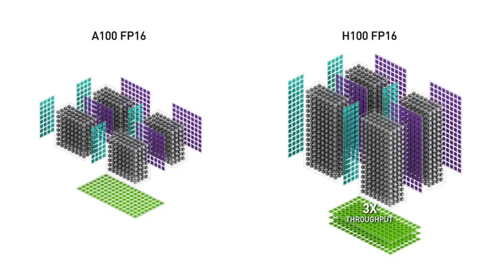
The H100 is equipped with fourth-generation Tensor Cores, which are significantly faster than the third-generation cores in the A100. According to NVIDIA the cores offer up to 6x the chip-to-chip speed, including per-SM (Streaming Multiprocessor) speedup, an increased count of SMs, and higher clocks. Specifically, they deliver double the Matrix Multiply-Accumulate (MMA) computational rates on equivalent data types and quadruple the rate using the new FP8 data type.
New Architectural Features
DPX Instructions: These accelerate dynamic programming algorithms by up to 7x compared to the A100, enhancing applications like genomics processing and optimal routing for robots.
Thread Block Cluster: This new feature allows for programmatic control over groups of thread blocks across multiple SMs, enhancing data synchronization and exchange, a significant step up from the A100's capabilities.
Distributed Shared Memory and Asynchronous Execution: These features enable direct SM-to-SM communications and efficient data transfers, which are improvements over the A100's architecture.
Transformer Engine: Customized for the H100, this engine optimizes transformer model training and inference, managing calculations more efficiently and boosting AI training and inference speeds dramatically compared to the A100.
Memory and cache improvements
The H100 introduces HBM3 memory, providing nearly double the bandwidth of the HBM2 used in the A100. It also features a larger 50 MB L2 cache, which helps in caching larger parts of models and datasets, thus reducing data retrieval times significantly.
Interconnectivity and scalability
Enhanced NVLink and NVSwitch technologies in the H100 offer substantial bandwidth increases, supporting more extensive and efficient GPU clustering capabilities compared to the A100. The new NVLink Switch System also allows for a more expansive and isolated GPU network.
Multi-Instance GPU (MIG)
The second-generation MIG technology in the H100 provides more compute capacity and memory bandwidth per instance, along with new confidential computing capabilities that secure user data and operations more robustly than the A100.
These improvements make the H100 not just a successor to the A100 but a substantially more powerful and versatile platform, especially suited for the most demanding AI applications and data-intensive tasks.
How to compare H100 and A100 performance
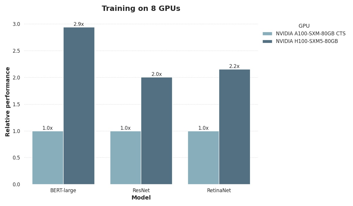
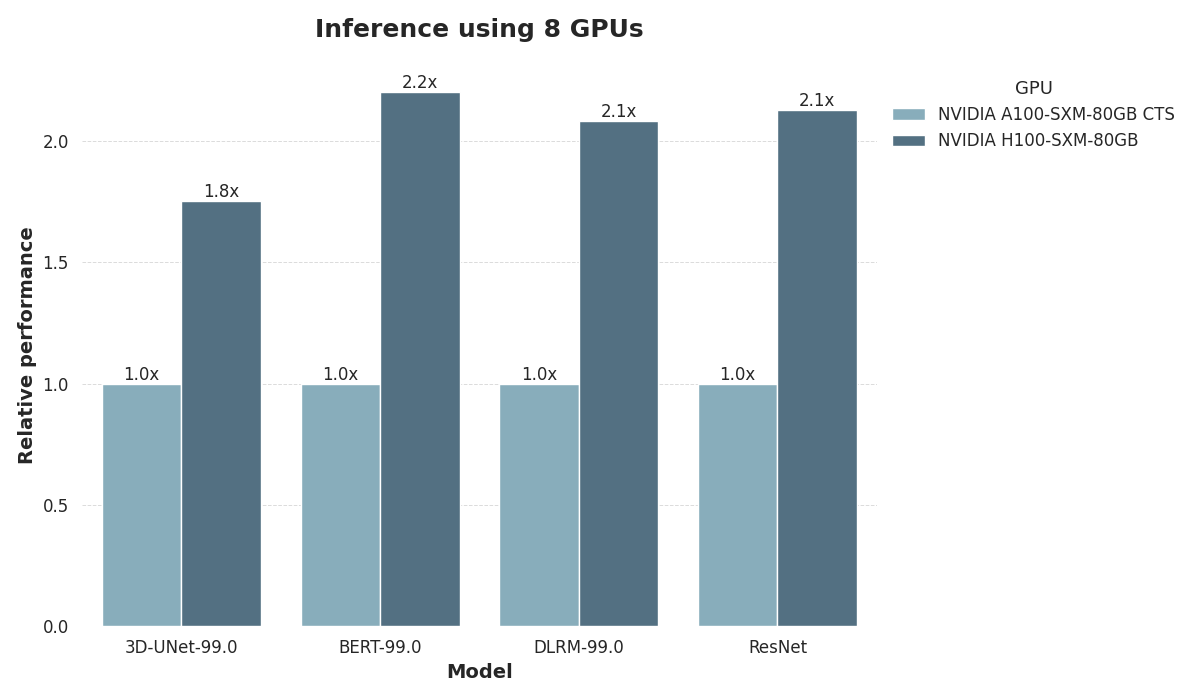
To compare A100 and H100, we evaluated their performance on the MLPerf training and MLPerf-Inference-Datacenter 3.0 machine learning benchmarks.
We evaluated training performance using three models:
The PLM BERT-Large,
The ResNet v1.5 vision model, and
The RetinaNet object recognition model.
When training, we used configurations with 8 GPUs, each equipped with 80 GB of memory.

We examined inference speed using four different models:
The PLM BERT-Large,
The recommendation model DLRM,
The volumetric segmentation model 3D-UNet, and
The ResNet v1.5 vision model.
During inference, we used configurations with 8 GPUs, each equipped with 80 GB of memory.

Both training and inference demonstrate a substantial performance gap between A100 and H100, with H100 regularly delivering double inference and training speed compared to A100. When training BERT-Large, performance in fact triples compared to A100. This underscores the large differences between the Hopper and Ampere architectures.
Superior AI performance with H100
The H100 is specifically engineered for optimal performance in AI and ML workloads. It introduces new SMs (Streaming Multiprocessors) that deliver higher throughput and efficiency. For AI developers, this means quicker model training times and more efficient inference computations, particularly with the most demanding AI models.
Versatility and consistency with A100
While the A100 may not match the H100 in raw AI-specific enhancements, its robust performance across diverse computing tasks makes it a reliable choice for many developers. The A100's ability to handle various precision formats (FP32, FP64, etc.) with high efficiency ensures that it remains a top contender for tasks that require a balance of accuracy and speed.
GPU Performance | NVIDIA A100 | NVIDIA H100 PCIe | NVIDIA H100 SXM5 |
|---|---|---|---|
Peak FP16 Tensor TFLOPS | 312/624^2 | 800/1600^2 | 1000/2000^2 |
Peak FP16 Tensor TFLOPS | 312/624^2 | 800/1600^2 | 1000/2000^2 |
Peak TF32 Tensor TFLOPS | 156/312^2 | 400/800^2 | 500/1000^2 |
Peak FP64 Tensor TFLOPS | 19.5 | 48 | 60 |
Peak INT32 TOPS | 19.5 | 24 | 30 |
Performance per Watt: A Closer Look at FP16 Efficiency
When comparing the NVIDIA H100 and A100 GPUs, performance per watt is a crucial metric for evaluating efficiency, particularly for AI workloads that rely heavily on FP16 precision. Both GPUs excel in delivering high computational throughput, but the H100’s architectural advancements make it a clear leader in energy efficiency.
Power Consumption and FP16 Performance per Watt
GPU | Power Consumption | FP16 Performance per Watt |
|---|---|---|
NVIDIA A100 | Up to 400W | Up to 10 TFLOPS/W |
NVIDIA H100 | Up to 700W | Up to 20 TFLOPS/W |
The NVIDIA A100 delivers up to 10 TFLOPS/W at FP16 precision, achieving a peak FP16 throughput of 4000 TFLOPS under its maximum 400W power consumption. This was revolutionary upon release and remains a highly efficient option for machine learning tasks.
However, the NVIDIA H100 doubles the efficiency, achieving up to 20 TFLOPS/W at FP16 precision, with a peak FP16 throughput of 14,000 TFLOPS under its maximum 700W power envelope. This leap in efficiency stems from the Hopper architecture's improvements, such as 4th-generation Tensor Cores and support for sparsity, which accelerates matrix operations while conserving power.
Compare cost of H100 and A100
When you compare the cost of the NVIDIA H100 and A100 it’s important to remember that these are both premium cloud GPUs aimed at demanding AI workloads. The availability of both GPUs is limited to the consumer market and your best option is to go with a cloud GPU platform provider like DataCrunch.
Current* On-demand price of NVIDIA H100 and A100:
Cost of H100 SXM5: $2.65/hour.
Cost of A100 SXM4 80GB: $1.65/hour.
Cost of A100 SXM4 40GB: $1.29/hour. * see real-time price of A100 and H100.
When you’re evaluating the price of the A100, a clear thing to look out for is the amount of GPU memory. In the case of the A100 you can see both 40GB and 80GB options available, and the smaller option may not be suitable for the largest models and datasets.
Another thing that makes comparing H100 and A100 costs difficult is that both GPUs are offered with different form factors, the SXM and PCIe. For demanding AI workloads, the SXM offers a substantial advantage.
Making the choice: H100 or A100?
Deciding between the H100 and A100 will largely depend on specific project requirements:
For AI testing, training and inference that demands the latest in GPU technology and specialized AI optimizations, the H100 can be the better choice. Its architecture is capable of the highest compute workloads and future-proofed to handle next-generation AI models and algorithms.
For mixed workloads and environments where cost-efficiency, versatility, and robust performance across a variety of applications are valued, the A100 continues to be a good option. Its MIG capabilities and broad applicability make it ideal for data centers and enterprises with diverse computational needs.
NVIDIA’s H100 and A100 GPUs both offer powerful options for AI developers, but the best choice depends on the specific demands of your projects. At DataCrunch we offer both H100 SXM5 and A100 SX4 on-demand, so spin up an instance and try for yourself.
