The NVIDIA A100 Tensor Core is a beast of a GPU. Launched in 2020, the A100 represented a massive leap forward in terms of raw compute power, efficiency, and versatility for high-performance machine learning applications.
Role of A100 GPU Today
Throughout the past four years the A100 has been the go-to GPU for accelerating complex computations, enabling breakthroughs in fields ranging from natural language processing to deep learning and scientific simulations.
With the introduction of the H100 the A100 has been surpassed in terms of raw performance, scalability, and feature set. Despite this, the A100 remains a powerful tool for AI engineers and data scientists because of its robust capabilities, better availability and proven track record.
A100 Specs and Performance Overview
Let's go through the NVIDIA A100 GPU in detail. We’ll review architecture, new features, performance specs and memory configurations.
Let’s also compare the A100 with its predecessor, the V100, and its successors, the H100 and the H200. Finally, we’ll go through some use cases where the A100 has made a significant impact, particularly in AI training and inference.
A100 Data Sheet Comparison vs V100 and H100
GPU Features | NVIDIA V100 | NVIDIA A100 | NVIDIA H100 SXM5 |
|---|---|---|---|
GPU Board Form Factor | SXM2 | SXM4 | SXM5 |
SMs | 80 | 108 | 132 |
TPCs | 40 | 54 | 66 |
FP32 Cores / SM | 64 | 64 | 128 |
FP32 Cores / GPU | 5020 | 6912 | 16896 |
FP64 Cores / SM (excl. Tensor) | 32 | 32 | 64 |
FP64 Cores / GPU (excl. Tensor) | 2560 | 3456 | 8448 |
INT32 Cores / SM | 64 | 64 | 64 |
INT32 Cores / GPU | 5120 | 6912 | 8448 |
Tensor Cores / SM | 8 | 4 | 4 |
Tensor Cores / GPU | 640 | 432 | 528 |
Texture Units | 320 | 432 | 528 |
Memory Interface | 4096-bit HBM2 | 5120-bit HBM2 | 5120-bit HBM3 |
Memory Bandwidth | 900 GB/sec | 1555 GB/sec | 3.35 TB/sec |
Transistors | 21.1 billion | 54.2 billion | 80 billion |
Max thermal design power (TDP) | 300 Watts | 400 Watts | 700 Watts |
* see detailed comparisons of V100 vs A100 and A100 vs H100.
NVIDIA A100 GPU Architecture
The NVIDIA A100 GPU is built on the Ampere architecture, which introduced several major improvements over its predecessor, the Volta architecture. The A100 includes 54 billion transistors, a significant increase from the 21 billion transistors in the V100.
Third-Generation Tensor Cores
One of the major features of the A100 is its third-generation Tensor Cores. These cores are designed to accelerate AI workloads by performing matrix multiplications and accumulations, which are obviously fundamental operations in deep learning models.
The third-generation Tensor Cores in the A100 support a broader range of precisions, including FP64, FP32, TF32, BF16, INT8, and more. This versatility allows the A100 to deliver optimal performance across various AI and HPC tasks.
Additionally, the A100 introduces support for structured sparsity, a technique that leverages the inherent sparsity in neural network models to double the throughput for matrix operations. This means that the A100 can process more data in less time, significantly speeding up training and inference times for AI models.
Multi-Instance GPU (MIG) Technology
Another major innovation in the A100 architecture is Multi-Instance GPU (MIG) technology. MIG allows a single A100 GPU to be partitioned into up to seven smaller, fully isolated instances. Each instance operates as an independent GPU, with its own dedicated resources such as memory and compute cores. This feature is particularly valuable in multi-tenant environments, such as data centers, where multiple users or applications can share the same physical GPU without interference.
MIG technology improves resource utilization and efficiency, enabling more flexible and cost-effective deployment of GPU resources. For instance, smaller AI inference tasks can run simultaneously on different MIG instances, maximizing the overall throughput of the A100 GPU.
NVLink 3.0
To support high-speed communication between GPUs, the A100 incorporates NVLink 3.0 technology. NVLink 3.0 provides a bi-directional bandwidth of 600 GB/s, allowing multiple A100 GPUs to work together seamlessly in a single system. This high-speed interconnect is crucial for large-scale AI and HPC applications that require massive amounts of data to be exchanged between GPUs in real-time.
PCIe and SXM4
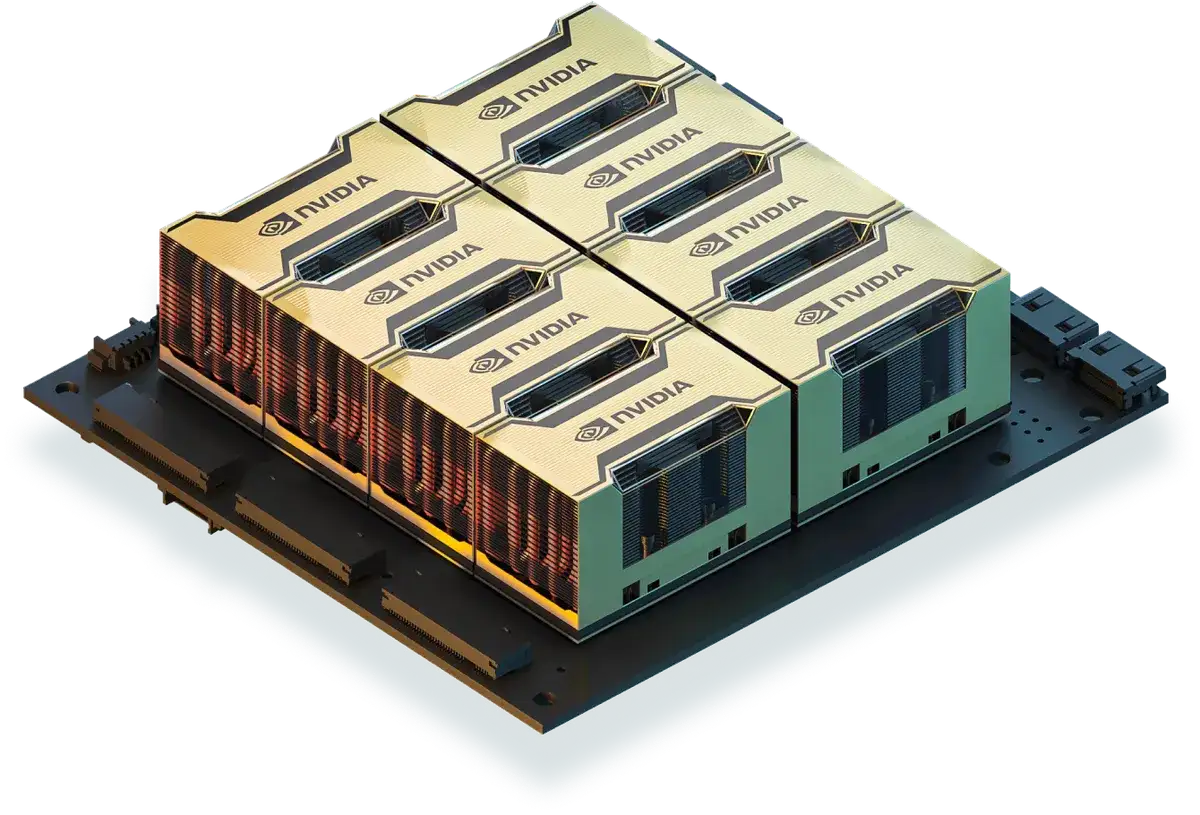
The A100 comes in two different socket form factors, the PCIe or SXM4. While PCIe can be a good option for more limited use cases, SXM brings considerable scalability and performance in large-scale machine learning training and inference.
Detailed A100 Performance Specs
The NVIDIA A100 GPU's performance is highlighted by its impressive computational power and advanced architectural features. Below, we break down the key performance specs that make the A100 a powerhouse for AI and HPC workloads.
Computational Performance
Precision Type | Peak Performance (TFLOPS/TOPS) |
|---|---|
FP64 (Double Precision) | 9.7 TFLOPS |
FP32 (Single Precision) | 19.5 TFLOPS |
TF32 (Tensor Float) | 156 TFLOPS |
FP16 (Half Precision) | 312 TFLOPS |
BFLOAT16 | 312 TFLOPS |
INT8 | 1,248 TOPS |
INT4 | 2,496 TOPS |
FP32 (Single Precision): The A100 delivers up to 19.5 TFLOPS of single-precision performance, making it highly effective for general-purpose computing tasks and AI training.
TF32 (TensorFloat-32): With the introduction of TF32 precision, the A100 achieves up to 156 TFLOPS, significantly accelerating AI training workloads without sacrificing accuracy.
FP16 (Half Precision): For tasks that can tolerate lower precision, such as neural network training, the A100 provides up to 312 TFLOPS of performance in FP16 mode.
INT8: Inference tasks often benefit from lower precision, and the A100 delivers up to 624 TOPS (Tera Operations Per Second) in INT8, facilitating rapid inference for AI models.
FP64 (Double Precision): For scientific computing and simulations requiring high precision, the A100 offers 9.7 TFLOPS of double-precision performance, essential for accurate results in HPC applications.
Memory and Bandwidth
Memory Capacity: Available in 40GB and 80GB configurations, the A100's HBM2e memory ensures ample capacity for large datasets and complex models.
Memory Bandwidth: With bandwidths of 1.6 TB/s (40GB) and 2 TB/s (80GB), the A100 ensures rapid data transfer between the GPU and memory, minimizing bottlenecks and enhancing overall performance.
Scalability
The A100's architecture supports seamless scalability, enabling efficient multi-GPU and multi-node configurations.
Multi-GPU Configurations: Using NVLink 3.0, multiple A100 GPUs can be interconnected to work together as a single unit. This increases computational power and memory capacity, allowing for larger and more complex workloads.
Multi-Node Clusters: For massive computational tasks, A100 GPUs can be deployed across multiple nodes in a cluster. High-speed interconnects like NVIDIA InfiniBand ensure efficient communication between nodes, enabling distributed training and large-scale simulations.
Software Ecosystem NVIDIA provides a comprehensive software ecosystem to support the deployment and scalability of A100 GPUs. Key components include:
CUDA: NVIDIA's parallel computing platform and programming model that enables developers to leverage the full power of A100 GPUs for their applications.
NVIDIA TensorRT: A high-performance deep learning inference library that optimizes AI models for deployment on A100 GPUs, ensuring maximum efficiency and performance.
NVIDIA NGC: A catalog of pre-trained AI models, SDKs, and other resources that help developers get started quickly with A100 GPUs. NGC also provides containers that simplify the deployment of AI and HPC applications.
NVIDIA Triton Inference Server: A scalable, multi-framework inference server that simplifies the deployment of AI models at scale, ensuring efficient utilization of A100 GPUs.
NVIDIA A100 Pricing
NVIDIA A100 Pricing
For a long time, the NVIDIA A100 was in extremely limited supply, making access to its compute power challenging. Today, availability has improved, and you can access both the A100 40GB and 80GB on-demand or by reserving longer-term dedicated instances.
Current Pricing for A100 Instances at DataCrunch
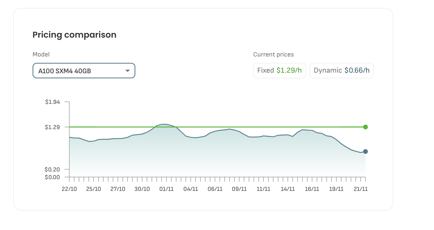
40 GB A100 SXM4
Fixed Pricing: $1.29/hour
Dynamic Pricing: $0.66/hour (market-driven, changes daily based on supply and demand)
80 GB A100 SXM4
Fixed Pricing: $1.65/hour
Dynamic Pricing: $1.42/hour (market-driven, changes daily based on supply and demand)
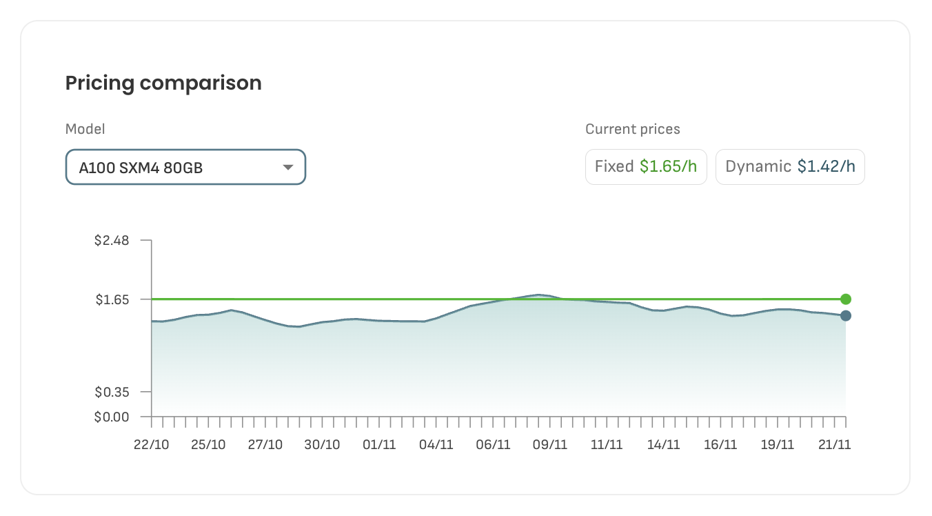
Dynamic pricing can be considerably less during off-peak times, allowing users to optimize their costs.
Real-time A100 prices can be found here.
Bottom line on the A100 Tensor Core GPU
Despite being surpassed in raw compute performance by the H100, the A100 is still one beast of a GPU. By enabling faster and more efficient computations, the A100 is still an extremely powerful enabler for AI training and inference projects. If you’re looking to try out the A100, spin up an instance with DataCrunch today.