
If you plan to use NVIDIA H100 GPUs for AI training or inference, you have a key decision to make with the socket form factor. Do you choose PCIe or do you need the extra performance of SXM?
Let’s review how the PCIe and SXM5 form factors of the NVIDIA H100 compare in specifications and performance.
Why H100 comes in PCIe and SXM5 form factors
Demand for high-performance GPUs is at an all-time high. It feels like everyone from enterprise companies to hyper-scalers to new AI startups are going after the same GPUs to feed their computational needs. As a response, NVIDIA has brought to market both PCIe and SXM form factors of the H100.
By giving more flexibility to different use-cases, NVIDIA has made the H100 the top performing GPU across many use-cases including high-performance computing (HPC) and AI training and inference.
What is PCIe?
PCIe (Peripheral Component Interconnect Express) is a high-speed interface standard used to connect various hardware components to a computer's motherboard. PCI was developed originally by Intel and introduced in 1992. PCIe (where "e" stands for express) was launched in 2003.
PCIe operates using lanes, which are pairs of wires that transfer data between the motherboard and the peripheral device. Each PCIe slot can have multiple lanes (x1, x4, x8, x16, etc.), with x16 being the most common for GPUs, providing the highest bandwidth.
What is SXM?
SXM is a custom socket form factor designed by NVIDIA specifically for high-performance computing and intense machine learning workloads. Originally introduced with the P100 GPUs in 2016, it offers higher density and performance by integrating GPUs more closely with the system board.
SXM stands for Server PCI Express Module. It is designed to work with NVIDIA’s NVLink interconnects for direct GPU-to-GPU communication with higher bandwidth, up to 900GB/s per connection. Up to 8 GPUs can be connected to a single SXM board.
H100 PCIe vs SXM5 Specifications Comparison
Feature | H100 PCIe | H100 SXM5 |
|---|---|---|
Form Factor | PCIe Gen 5 | SXM5 |
Memory Bandwidth | 2 TB/s | 3.35 TB/s |
L2 Cache | 50 MB | 50 MB |
Transistors | 80 billion | 80 billion |
GPU Memory | 80 GB | 80 GB |
Memory Interface | 5120-bit HBM2e | 5120-bit HBM3 |
Interconnect | NVLink: 600 GB/s PCIe Gen5 128 GB/s | - NVLink: 900 GB/s - PCIe Gen5 128 GB/s |
Max Thermal Design Power (TDP) | 300-350W | Up to 700W |
H100 PCIe Form Factor
The PCIe version of the H100 is designed to slot into standard server racks, making it a versatile option for many datacenters. It's a full-length, full-height, double-width card that you can easily integrate into existing infrastructure.
One of the standout features of the H100 PCIe is its support for PCIe Gen 5. This latest standard offers significantly improved bandwidth over previous generations of GPUs like the A100 or V100, allowing up to 120 GB/s transfer speeds between the GPU and the rest of your system.
Many of the H100 PCIe form factor elements are identical to SXM, including 80 billion transistors, 50 MB L2 Cache and 80GB GPU memory. The PCIe version of H100 comes with HBM2e memory interface and has a lower 2 TB/s memory bandwidth and 300-350 Thermal Design Power.
H100 SXM5 Form Factor
The SXM5 module is designed to be directly integrated into specialized server boards. With a 5120-bit HBM3 memory interface H100 SXM5 is capable of up to 3.35 TB/s memory bandwidth.
It supports NVIDIA's fourth-generation NVLink technology allowing for 900GB/s GPU-to-GPU interconnect bandwidth. When combined with the third-generation NVSwitch, you can create incredibly powerful multi-GPU systems that leverage a higher 700W maximum TDP.
H100 PCIe vs SXM5 Performance Comparison
| NVIDIA H100 PCIe | NVIDIA H100 SXM5 |
|---|---|---|
Peak FP64 | 24 TFLOPS | 30 TFLOPS |
Peak FP64 Tensor Core | 48 TFLOPS | 60 TFLOPS |
Peak FP32 | 48 TFLOPS | 60 TFLOPS |
Peak FP16 | 96 TFLOPS | 120 TFLOPS |
Peak BF16 | 96 TFLOPS | 120 TFLOPS |
Peak TF32 Tensor Core | 400 TFLOPS | 800 TFLOPS* | 500 TFLOPS | 1000 TFLOPS* |
Peak FP16 Tensor Core | 800 TFLOPS | 1600 TFLOPS* | 1000 TFLOPS | 2000 TFLOPS* |
Peak BF16 Tensor Core | 800 TFLOPS | 1600 TFLOPS* | 1000 TFLOPS | 2000 TFLOPS* |
Peak FP8 Tensor Core | 1600 TFLOPS | 3200 TFLOPS* | 2000 TFLOPS | 4000 TFLOPS* |
Peak INT8 Tensor Core | 1600 TOPS | 3200 TOPS* | 2000 TOPS | 4000 TOPS* |
*with sparsity.
The peak performance specs of the SXM5 are not substantially better than the PCIe. The major difference comes when you leverage the NVLink technology and 900 GB/s interconnect to allow up to 8 H100 SXM GPUs to function effectively as one massive GPU.
For large language model training where more than one GPU is likely to be used the SXM5 version performs considerably better than the PCIe. In memory-intensive workloads like AI model training the 3.35 TB/s memory bandwidth of the SXM5 also results in much faster training speeds.
H100 PCIe vs. SXM5 in the MLPerf benchmark
To illustrate the performance gap between the SXM5 and PCIe form factors, we evaluated their inference performance on the MLPerf machine learning benchmark, focusing on two popular tasks:
LLM inference using the Llama 2 70B LoRA model, and
Image generation using Stable Diffusion XL.
For both tasks, we used configurations with 8 GPUs, each equipped with 80 GB of memory.
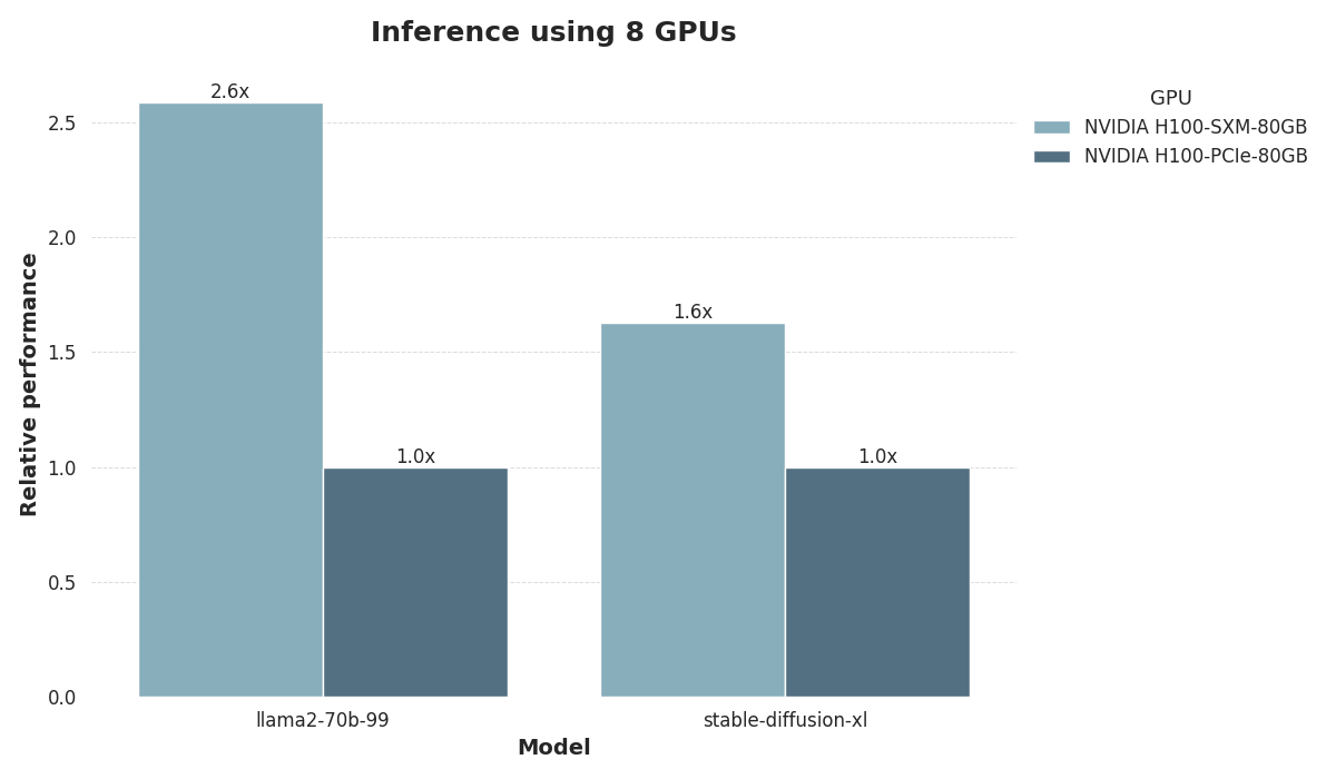
The results clearly demonstrate the advantages of the SXM5 form factor. SXM5 delivers a striking 2.6x speedup on LLM inference compared to PCIe. On image generation, SXM5 still outperforms PCIe by 1.6x, though the performance gap is less pronounced. These findings underscore the SXM5’s significant edge over PCIe, particularly with large modern deep learning models.
H100 SXM5 Use Cases
The SXM5 version of the H100 is ideally suited for high-performance computing (HPC) and large-scale AI training workloads that demand the absolute peak of GPU performance. It thrives in multi-GPU computational scaling and high-bandwidth inter-GPU communications.
For HPC applications the SXM5's superior performance in tasks like lattice QCD and 3D FFT makes it the top choice. The ability to leverage NVLink for fast GPU-to-GPU communication can significantly accelerate complex scientific computations that require frequent data exchange between GPUs.
In AI training and inference related use-cases, the SXM5 is much more powerful when training massive AI models, particularly in natural language processing. For instance, when working with very large language models, the SXM5's enhanced multi-GPU scaling capabilities can dramatically reduce training times.
The SXM5 is also well-suited for AI applications that require processing enormous datasets or handling multiple AI tasks simultaneously. Its higher memory bandwidth and better scaling make it optimal for these data-intensive, computationally complex workloads.
DataCrunch exclusively uses SXM technology on the A100 and H100 GPU series.
H100 PCIe Use Cases
The PCIe version of the H100, while still extremely powerful, is better suited for more flexible and diverse deployment scenarios. It's an excellent choice for organizations that need to upgrade their existing infrastructure without a complete overhaul of their server architecture.
For AI inference workloads, particularly those that don't require extensive multi-GPU communication, the PCIe version can offer balance of performance and cost-effectiveness. It's well-suited for deploying production AI models in scenarios like recommendation systems, natural language understanding, or computer vision applications where single-GPU performance is good enough.
The PCIe form factor could also be suitable for smaller-scale AI training tasks or for organizations that need to distribute their compute resources across multiple locations. For instance, it's a good fit for edge computing scenarios where powerful GPU compute is needed closer to the data source, such as in smart manufacturing plants or autonomous vehicle testing facilities.
Bottom Line on PCIe vs SXM5
Ultimately, the choice between SXM5 and PCIe depends on your performance needs, infrastructure, scalability requirements, and budget. The SXM5 offers superior performance for the most demanding workloads, while the PCIe provides a more flexible, widely compatible option that still delivers impressive performance across a broad range of AI and HPC applications.
Let’s end with some good news. Availability of NVIDIA’s Tensor Core GPUs like the A100 and H100 is improving on premium cloud GPU platforms. You don’t need to make a massive infrastructure investment to test out the capability of one or more H100 for your needs. Spin up an instance with DataCrunch or reach out for a tailored quote.